Nanofilm’s Participation in Guhring Grinding Competence Center Open House
- 05 Mar, 2025
Media Contact
Categories
As the semiconductor industry progresses, there is a clear shift towards larger wafer sizes, such as 300mm, 450mm, and beyond. This shift places increased demands on critical components in the back-end processing stages, particularly lapping carriers, which must adhere to stricter precision requirements and higher performance standards. These evolving demands underscore the lapping carrier PVD coating challenges in semiconductor manufacturing, where traditional methods struggle to meet the new performance benchmarks.
Traditional DLC coatings, commonly applied using PVD coating for semiconductor and PECVD methods, have served the industry well, but with the increasing size and fragility of wafers, the challenges of achieving high precision, uniformity, and edge protection are becoming more pronounced. As a result, the need for an advanced coating for semiconductor manufacturing has never been greater. Today’s wafer processing environment requires coatings that can perform reliably under extreme conditions while maintaining wafer yield and minimizing operational costs.
Understanding the Role of Lapping Carriers in Semiconductor Manufacturing
What is a Lapping Carrier?
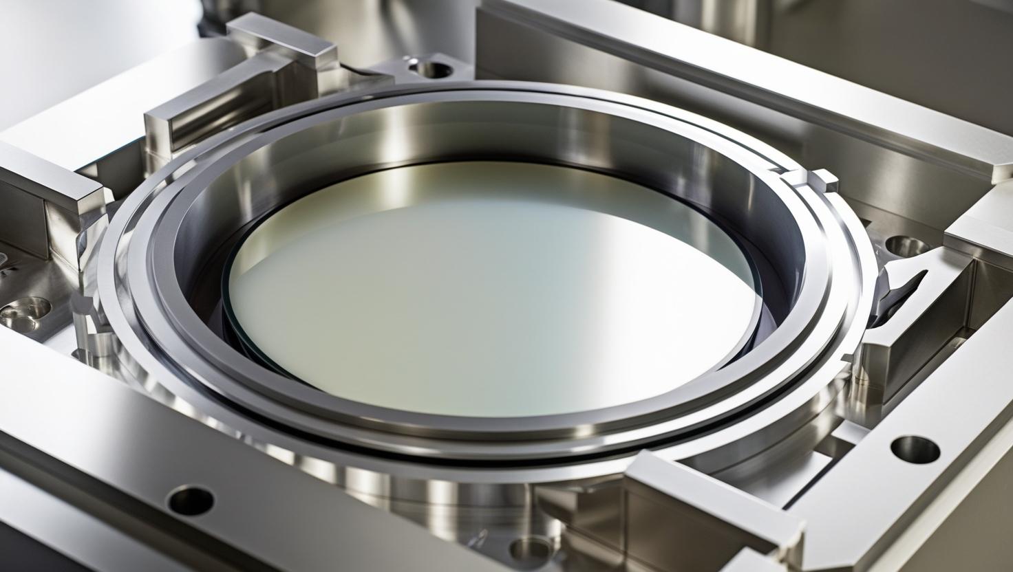
A lapping carrier, also known as a workholder or polishing carrier, is a precision-engineered component used to securely hold semiconductor wafers during double-sided lapping and polishing. These carriers play a crucial role in ensuring the uniform material removal required for achieving ultra-smooth wafer surfaces.
Importance of Lapping Carriers in Semiconductor Back-End Processing
Lapping carriers are integral to the wafer thinning and polishing stages of semiconductor manufacturing. These steps occur after front-end processes such as lithography and etching, preparing the wafer for dicing and packaging.
Key Functions:
- Wafer Thinning: Securely holds wafers while reducing thickness to meet device packaging specifications.
- Chemical Mechanical Planarization (CMP): Ensures uniform polishing to achieve a flat, defect-free wafer surface.
- Edge Protection: Prevents chipping or damage to delicate wafers during high-precision polishing.
As semiconductor node sizes shrink and wafer sizes increase, the demand for high-performance lapping carriers with advanced coatings becomes even more critical.
Key Insights on Lapping Carriers & Challenges:
1. Larger Wafer Sizes Require Enhanced Precision:
As wafer sizes grow, maintaining uniform thickness, flatness, and edge protection becomes increasingly difficult. Lapping carriers play a crucial role in achieving these tight tolerances, which is essential for high-value wafers.
2. Total Thickness Variation (TTV) Concerns:
The need for lapping carriers that reduce TTV is heightened by the size of modern wafers. Proper rotation freedom provided by lapping carriers ensures uniform material removal, crucial for maintaining wafer quality.
3. Edge Protection for Fragile Wafers:
With the larger size and fragility of wafers, edge protection becomes a more critical issue. Lapping carriers prevent edge damage during the delicate polishing process, ensuring higher-quality wafers.
4. Rising Semiconductor Demand:
The increasing demand for advanced semiconductors in industries like AI, electric vehicles, and industrial automation has led to greater production volumes of larger wafers. This necessitates a more reliable and efficient lapping carrier solution to meet both precision and yield requirements.
DLC Coatings in Lapping Carriers: Types and Applications
What is DLC Coating and Why is it Used in Lapping Carriers?
Diamond-Like Carbon (DLC) coatings are a family of amorphous carbon coatings that exhibit properties similar to diamond, such as high hardness, low friction, and superior wear resistance. These coatings are essential for lapping carriers because they:
- Reduce friction to minimize wafer surface defects.
- Enhance wear resistance, extending carrier lifespan.
- Improve chemical resistance against aggressive polishing slurries.
- Maintain process stability with consistent coating performance.
Common DLC Coatings Used in Lapping Carriers
DLC coatings for semiconductor lapping carriers are primarily deposited using PVD (Physical Vapor Deposition) and PECVD (Plasma-Enhanced Chemical Vapor Deposition) technologies.
1. PVD-Based DLC Coatings:
- Deposited via sputtering or cathodic arc methods.
- Offer high hardness and good adhesion.
- May suffer from residual stresses, leading to adhesion failures over time.
2. PECVD-Based DLC Coatings:
- Typically hydrogenated amorphous carbon (a-C:H).
- Provide good step coverage on complex geometries.
- More susceptible to wear and chemical degradation in aggressive polishing environments.
Challenges Faced with PVD and PECVD DLC Coatings in Lapping Carriers
Despite their benefits, PVD and PECVD coatings are increasingly struggling to meet the demands of modern semiconductor manufacturing. Some of the major challenges include:
1. Adhesion Failures:
- PVD coatings often exhibit high residual stress, leading to delamination.
- PECVD coatings may have weaker substrate bonding, reducing longevity under high loads.
2. Wear and Abrasion Issues
- Increased wafer throughput accelerates coating wear and thinning.
- Hard DLC coatings tend to become brittle, leading to micro-cracking.
3. Chemical Degradation
- Advanced polishing slurries used in CMP processes degrade DLC coatings over time.
- PECVD coatings are more vulnerable to etching and oxidation, reducing carrier lifespan.
4. Increased Wafer Sizes and Higher Process Pressures
- Larger wafers (300mm+) require stronger adhesion and better mechanical durability.
- Traditional coatings struggle to maintain uniform coverage and stress resistance.
5. Cost Pressures and Downtime
- Frequent carrier recoating or replacements increase operational costs.
- Coating failures and related defects lead to downtime and potentially reduced yield by 0.5%-2%, impacting overall efficiency.
The FCVA-Based TAC-ON Coating Solution
Addressing the Challenges of PVD and PECVD DLC Coatings
Traditional DLC coatings applied via PVD and PECVD face significant challenges in semiconductor wafer lapping carriers, including poor adhesion, high wear rates, friction-related contamination, and delamination under stress. These issues lead to frequent replacements, increased operational costs, and lower production efficiency.
FCVA-based TAC-ON® coatings provide a superior alternative, overcoming these challenges through advanced deposition technology and optimized material properties.
How TAC-ON® Coatings Solve These Problems
1. Superior Hardness and Wear Resistance
- Problem with PVD/PECVD DLC: Lower hardness (~15 GPa) results in faster wear, leading to frequent replacements and increased downtime.
- TAC-ON Solution: With a hardness of ~40 GPa, TAC-ON coatings are significantly more wear-resistant, extending the lifespan of lapping carriers and reducing the need for frequent recoating or replacements.
2. Enhanced Adhesion and Delamination Resistance
- Problem with PVD/PECVD DLC: Poor adhesion leads to coating delamination under mechanical stress or prolonged usage, causing wafer contamination and rework.
- TAC-ON Solution: FCVA technology ensures superior adhesion, preventing delamination even under extreme operating conditions, reducing contamination risks, and improving yield rates.
3. Lower Friction and Reduced Contamination
- Problem with PVD/PECVD DLC: Higher friction coefficients (~0.14) increase wear debris, leading to surface contamination and defects in wafer processing
- TAC-ON Solution: With a friction coefficient of ~0.1, TAC-ON provides smoother operations, reducing contamination risks and improving overall wafer quality.
4. Uniform Coating at Low Temperatures
- Problem with PVD/PECVD DLC: High deposition temperatures can induce residual stress, leading to cracking and non-uniform coatings.
- TAC-ON Solution: The FCVA process allows uniform deposition at low temperatures, minimizing internal stress and ensuring consistent thickness, reducing defects such as pinholes and cracks.
Comparison: TAC-ON vs. Traditional DLC Coatings
| Property | TAC-ON (ta-C, FCVA) | Traditional DLC (PVD, PECVD) |
| Diamond Content (%) | ~85 | ~25 |
| Hardness (GPa) | ~40 | ~15 |
| Wear Rate (mm³/Nm) | <10⁻⁸ | ~8×10⁻⁸ |
| Friction Coefficient | ~0.1 | ~0.14 |
| Typical Thickness (nm) | ~1,200 | ~2,000 |
The Business Impact of Upgrading to TAC-ON Coating
1. Cost Efficiency and Reduced Downtime
- Thinner yet more durable: TAC-ON (~1,200 nm) requires less material than traditional DLC (~2,000 nm), reducing coating costs.
- Longer service life: Less frequent replacements mean lower maintenance costs and reduced production disruptions.
2. Higher Yield and Productivity
- Minimized contamination: Reduces wafer defects, improving yield rates and reducing costly rework.
- Lower friction and debris generation: Ensures cleaner processing environments, reducing scrap rates.
2. Scalability and Precision
- Tighter tolerances: A thinner, harder coating ensures minimal dimensional changes, maintaining high-precision performance.
- Better adaptability: More flexible for different lapping carrier models and specifications.
Conclusion
TAC-ON coatings offer a revolutionary alternative, providing superior adhesion, wear resistance, and contamination protection. Through Filtered Cathodic Vacuum Arc (FCVA) technology, these coatings are designed to address the challenges faced by lapping carriers in today’s high-precision wafer processing environments. By improving durability and performance, TAC-ON coatings help increase wafer yield and reduce operational costs, positioning manufacturers for success in an increasingly competitive semiconductor landscape.